Biography
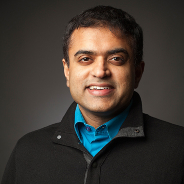
Debdeep Jena is the David E. Burr Professor of Engineering at Cornell University. He is in the departments of Electrical and Computer Engineering and Materials Science and Engineering, and is a field member in the department of Applied and Engineering Physics. He joined Cornell in 2015 from the faculty at Notre Dame where he was since August 2003, shortly after earning the Ph.D. in Electrical and Computer Engineering from the University of California, Santa Barbara (UCSB).
His teaching and research are in the quantum physics of semiconductors and electronic and photonic devices based on quantized semiconductor structures (e.g. Nitrides, Oxides, 2D Materials), and their heterostructures with superconductors, ferroelectrics and magnets, with device applications in energy-efficient transistors, light-emitting diodes and RF and power electronics and quantum computation and communications. His research is driven by the goal to enable orders of magnitude increase in the energy efficiency and speed for computation, memory, communications, lighting, and electrical energy management ranging from the chip to the grid.
The research from his group has been published in more than 300 journal papers including in Science, Nature, Physical Review Letters, Applied Physics Letters and Electron Device Letters. Several patents have been granted for the group’s research work. He is a fellow of the American Physical Society and is the winner of teaching awards and research awards such as the ISCS young scientist award in 2012, MBE young scientist award in 2014, and awards from the industry such as the IBM faculty award in 2012, and most recently the Intel Outstanding Research award in 2020.
Research Interests
The Jena group explores the fundamental limits of computation, memory, and communications with semiconductor devices by exploiting and understanding new physics. In recent years, they are immersed in research on the following topics:
- the performance limits of ultrahigh speed GaN and AlN transistors for all-electronic THz sources,
- ultra wide bandgap semiconductor transistors for power electronics (see Energy.gov presentation),
- photonic devices in the IR & visible, and deep-UV LEDs and lasers approaching 200 nm using quantum dots,
- ultra-low power electronics: logic and memory exploiting spintronics, topological insulators, and superconductors, and
- novel materials and devices for quantum computation and communication that go far beyond classical device limits.
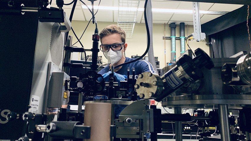
Often this research path requires us to explore new materials. We grow the new materials by ourselves using Molecular Beam Epitaxy (MBE), or work very closely with groups that do. Currently the materials families we are investigating for the above devices are:
- Nitride semiconductors (and nitride superconductors, magnets, and ferroelectrics),
- Graphene, hBN & 2D Crystals, and
- Oxide semiconductors, ferroelectrics, and multiferroics.
The goal to make devices also requires, or results in, a deep theoretical understanding of electron transport, electron-phonon interactions, light-matter interactions, geometric and topological aspects of condensed matter physics, and correlated electron physics. We do a significant amount of theory and modeling ourselves, and often also work closely with theoreticians.
Categorized research pages: Nitride Electronics, Oxide Electronics, UV Lasers/Photonics, 2D Materials, Ultrapolar/Ferro Semiconductors, Super/Semi Electronics
Research Group MembersSelected Publications
- P. Dang et al., “An all-epitaxial nitride heterostructure with concurrent quantum Hall effect and superconductivity”, Science Advances 7, eabf1388 (2021)
- K. Nomoto et al., “GaN/AlN p-channel HFETs with Imax>420 mA/mm and ~20 GHz fT/fMax”, IEDM (2020)
- R. Chaudhuri, S. Bader, Z. Chen, D. Muller, H. Xing, and D. Jena, “A polarization-induced 2D hole gas in undoped gallium nitride quantum wells”, Science 365, 1454 (2019)
- R. Yan et al., “GaN/NbN epitaxial semiconductor/superconductor heterostructures”, Nature 555, 183 (2018)
- S. Kim et al., “High-mobility and low-power thin-film transistors based on multilayer MoS2 crystals”, Nature Communications 3, 1022 (2012)
- J. Simon et al., “Polarization-Induced Hole Doping in Wide-Bandgap Uniaxial Semiconductor Heterostructures”, Science 327, 60 (2010)
- D. Jena and A. Konar, “Enhancement of Carrier Mobility in Semiconductor Nanostructures by Dielectric Engineering”, Physical Review Letters 98, 136805 (2007)
Selected Awards and Honors
- Intel Outstanding Researcher Award (2020)
- David Burr Chair Professor of Engineering (2020)
- Fellow, American Physical Society (2016)
- MBE Young Scientist Award (2014)
- IBM Faculty Award (2012)
- Young Scientist Award (International Symposium of Compound Semiconductors) (2012)
- Joyce award for excellence in undergraduate teaching (2010)
- NSF Career Award (2006)
Education
- B.S.(Electrical Engineering),Indian Institute of Technology,1998
- Ph.D.(Electrical and Computer Engineering),University of California,2003
Research Group Members
Graduate Students


